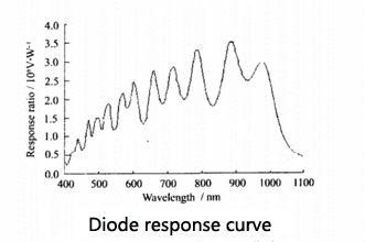
The figure above is the response curve of the silicon photodiode measured before the scintillation crystal is pasted.
The device's response rate oscillates because the surface of the device such as SiO2, PSG, and BSG is too thick and the light interferes. Redesigning the process steps or using additional processes, thinning the surface film thickness of the device will smooth the curve. After simulation, when the surface of the device has only a SiO2 film with a thickness of 0.2um, the film will be transparent to the 560nm fiber, which will improve the response rate of the device to the CsI(TI) scintillator.
In addition, as seen from the above figure, the response peak of the diode is 800---900 nm, and the relative response rate at 560 nm is only about 50%. Therefore, properly reduce the junction depth, select the appropriate dopant and surface concentration, avoid the "dead layer" with extremely short life caused by the diffusion of the magazine, improve the surface quality, and reduce the surface recombination by passivation or other processes. The speed can enhance the correspondence of the diode to the short-wave fiber, which will help improve the spectral response matching between the diode and the crystal, thereby enhancing the readout signal.
-
 Sales@hata-ndt.com
 -
 0086-0371-86172891